High Throughput Ethernet ASICs by Justin Pietsch
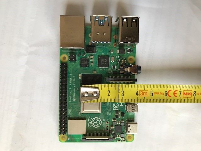 My Raspberry’s chip size: 10x10 mm
High-throughput Ethernet ASICs (Application-Specific Integrated Circuits) are a critical component of modern high-speed networking. In this post, I summarize key insights from Justin Pietsch’s article, “A Summary of High-Speed Ethernet ASICs,” and share some additional notes.
Key Takeaways from the Article
- Chip Reticle Limit: The absolute maximum size is 33x26 mm (858mm²). Nvidia’s next-gen chip, GA100, boasts 54.2 billion transistors and a die size of 826mm² using a 7nm processor node.
- Comparison to Raspberry Pi: For perspective, my Raspberry Pi’s chip is just 10x10 mm.
- ASICs vs GPUs: Network ASICs are now as large as GPUs, indicating the increasing complexity of networking hardware.
- Integrated Circuits (ICs): In this context, IP refers to “Intellectual Property.”
- Programmable Pipeline: The author argues that a programmable pipeline, especially for OpenFlow, may not be necessary.
- Vendor Considerations: The author expresses caution in using Cisco, as they lack experience in this area. However, there’s confidence in the Dune/Leaba team.
Key Quote to Remember
“As networks get large, the cost of the network is driven by the cost of the optics. The real money saving is not when you get a faster chip, but when the chip supports higher throughput SERDES.”
— Justin Pietsch